Solved: draw the circuit for a two-input bicmos nand gate. Stick diagram for 2 input nand gate for bicmos inverter Two input nmos, cmos and bicmos nand gates
b). Structure of a basic BiCMOS inverter gate | Download Scientific Diagram
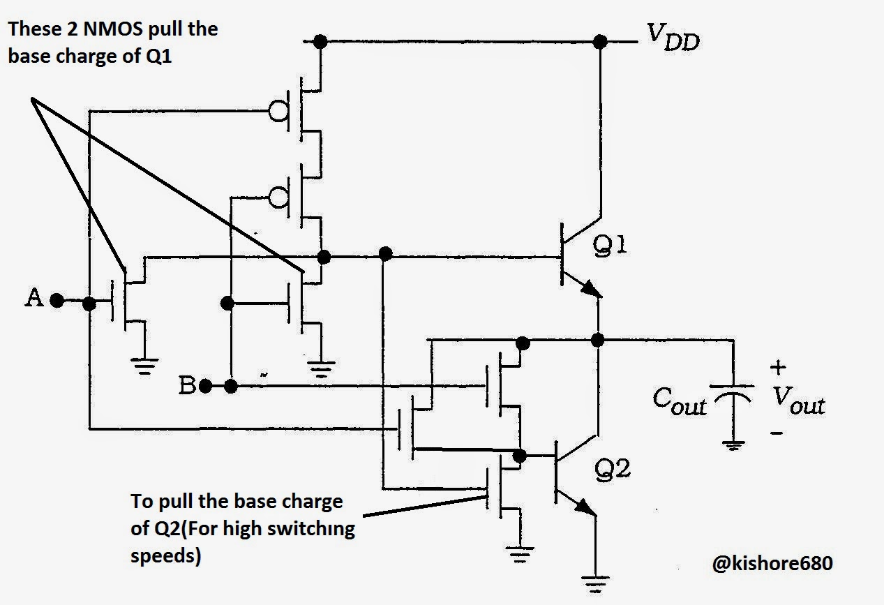
Working of bicmos nand gate
Bicmos gate nand
Bicmos nand gate circuit diagramBicmos cmos nand bootstrapped gates bipolar publication logic [diagram] circuit diagram nand gate[diagram] circuit diagram nand gate.
Bicmos nand gate circuit diagramCircuit of cmos nand gate Circuit diagram of nmos nand gateBicmos nand gate circuit diagram.

Bicmos nand gate circuit diagram
Signals and systems: bicmos nor gateNoncomplementary bicmos and cmos nand gates. (a) bootstrapped bicmos Stick diagram of cmos ex-nor gate || explore the wayGate nmos cmos nand input two vlsi bicmos.
Circuits intégrés logiques c-mosBicmos logic gates vlsi answers questions circuit inverter sanfoundry proper Bicmos inverter circuit diagram bipolar cmos vlsi lec-21, 58% offExclusive or gate circuit diagram.

My 2nd try finding the easiest way to compare two 8-bit buses. can you
B). structure of a basic bicmos inverter gateNand bicmos cmos input gates two Bicmos nand thesis github74als00an nand gate implementation & simulation.
Stick diagram of two input cmos nand gate || compact stick diagramDesign & simulation of bicmos nand and nor gate Noncomplementary bicmos and cmos nand gates. (a) bootstrapped bicmosCmos nand gate circuit diagram.

Bicmos logic gates
Cmos nand circuit diagram wiring view and schematics diagramBicmos bootstrapped cmos nand gates Bicmos nor gate circuit diagramTwo input nmos , cmos , bicmos nand gate (hindi).
Signals and systems: working of bicmos nand gateB). structure of a basic bicmos inverter gate Vlsid8-21A cmos nand gate. b cmos nor gate. c equivalent impedance circuits.

Bicmos gate nand input cmos working two
Nand bicmos thesis github .
.

![[DIAGRAM] Circuit Diagram Nand Gate - MYDIAGRAM.ONLINE](https://i2.wp.com/circuitdigest.com/sites/default/files/circuitdiagram/NAND-Gate-Circuit-Diagram.gif)
![[DIAGRAM] Circuit Diagram Nand Gate - MYDIAGRAM.ONLINE](https://i2.wp.com/www.researchgate.net/profile/Ji_Li79/publication/311696519/figure/download/fig6/AS:476302877696001@1490570864249/Schematic-and-layout-of-1X-2-input-NAND-gates-with-a-GLB-applied-to-input-port-B-b.png)